
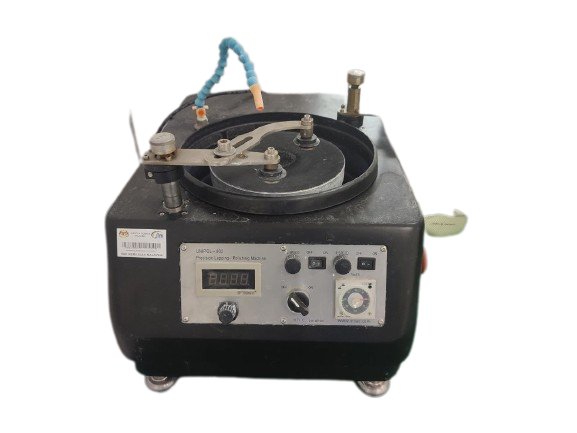
Lapping and Polishing are two types of method that are applied to wafers to obtain a very even and smooth surface of the consumables. Lapping is a mechanical process that uses a pad and polishing liquid to remove excess silicon from a wafer substrate, resulting in a dull-grey, semi-reflective surface. Lapping helps to erase flaws on the front and rear surfaces of the wafer while also decreasing stress that might accumulate during the ingot-slicing process. Polishing is a thermal-chemical-mechanical technique that decreases surface roughness on wafer substrates to achieve a mirror-like quality. Polishing on both sides produces wafers with the lowest TTV (Total Thickness Variation) values in the industry. Below is one of the wafer Lapping and Polishing system that our company provided to industries.
Interested to this product? Contact Us Now