The fabrication of an integrated circuit (IC) requires a variety of physical and chemical processes performed on a semiconductor (e.g., silicon) substrate. In general, the various processes used to make an IC fall into three categories: film deposition, patterning, and semiconductor doping.
Films of both conductors (such as polysilicon, aluminium, and more recently copper) and insulators (various forms of silicon dioxide, silicon nitride, and others) are used to connect and isolate transistors and their components. Selective doping of various regions of silicon allow the conductivity of the silicon to be changed with the application of voltage. By creating structures of these various components millions of transistors can be built and wired together to form the complex circuitry of a modern microelectronic device. Fundamental to all of these processes is lithography, i.e., the formation of three-dimensional relief images on the substrate for subsequent transfer of the pattern to the substrate.
Functionality
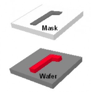
The importance of lithography can be appreciated in two ways. First, due to the large number of lithography steps needed in IC manufacturing, lithography typically accounts for about 30 percent of the cost of manufacturing. Second, lithography tends to be the technical limiter for further advances in feature size reduction and thus transistor speed and silicon area. Obviously, one must carefully understand the trade-offs between cost and capability when developing a lithography process. Although lithography is certainly not the only technically important and challenging process in the IC manufacturing flow, historically, advances in lithography have gated advances in IC cost and performance. Optical lithography is basically a photographic process by which a light sensitive polymer, called a photoresist, is exposed and developed to form three-dimensional relief images on the substrate. In general, the ideal photoresist image has the exact shape of the designed or intended pattern in the plane of the substrate, with vertical walls through the thickness of the resist. Thus, the final resist pattern is binary: parts of the substrate are covered with resist while other parts are completely uncovered. This binary pattern is needed for pattern transfer since the parts of the substrate covered with resist will be protected from etching, ion implantation, or other pattern transfer mechanism.
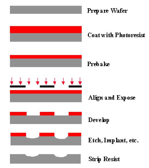
The general sequence of processing steps for a typical optical lithography process is as follows:substrate preparation, photoresist spin coat, prebake, exposure, post-exposure bake, development, and postbake.
A resist strip is the final operation in the lithographic process,after the resist pattern has been transferred into the underlying layer. This sequence is shown diagrammatically in Figure 1-1, and is generally performed on several tools linked together into a contiguous unit called a lithographic cluster. A brief discussion of each step is given below, pointing out some of the practical issues involved in photoresist processing. More on these topics will be discussed in detail in subsequent chapters
The basic principle behind the operation of a photoresist is the change in solubility of the resist in a developer upon exposure to light (or other types of exposing radiation). In the case of the standard diazonaphthoquinone positive photoresist, the photoactive compound (PAC), which is not soluble in the aqueous base developer, is converted to a carboxylic acid on exposure to UV light in the range of 350 – 450nm. The carboxylic acid product is very soluble in the basic developer. Thus, a spatial variation in light energy incident on the photoresist will cause a spatial variation in solubility of the resist in developer.