
What is Photolitography?
T he fabrication of an integrated circuit (IC) requires a variety of physical and chemical processes performed on a semiconductor (e.g., silicon) substrate. In general, the various processes used to make an IC fall into three categories: film deposition, patterning, and semiconductor doping. Films of both conductors (such as polysilicon, aluminium, and more recently copper) and insulators (various forms of silicon dioxide, silicon nitride, and others) are used to connect and isolate transistors and their components. Selective doping of various regions of silicon allow the conductivity of the silicon to be changed with the application of voltage. By creating structures of these various components millions of transistors can be built and wired together to form the complex circuitry of a modern microelectronic device. Fundamental to all of these processes is lithography, i.e., the formation of three-dimensional relief images on the substrate for subsequent transfer of the pattern to the substrate.
 The importance of lithography can be appreciated in two ways. First, due to the large number of lithography steps needed in IC manufacturing, lithography typically accounts for about 30 percent of the cost of manufacturing. Second, lithography tends to be the technical limiter for further advances in feature size reduction and thus transistor speed and silicon area. Obviously, one must carefully understand the trade-offs between cost and capability when developing a lithography process. Although lithography is certainly not the only technically important and challenging process in the IC manufacturing flow, historically, advances in lithography have gated advances in IC cost and performance.
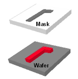
Optical lithography is basically a photographic process by which a light sensitive polymer, called a photoresist, is exposed and developed to form three-dimensional relief images on the substrate. In general, the ideal photoresist image has the exact shape of the designed or intended pattern in the plane of the substrate, with vertical walls through the thickness of the resist. Thus, the final resist pattern is binary: parts of the substrate are covered with resist while other parts are completely uncovered. This binary pattern is needed for pattern transfer since the parts of the substrate covered with resist will be protected from etching, ion implantation, or other pattern transfer mechanism.
The importance of lithography can be appreciated in two ways. First, due to the large number of lithography steps needed in IC manufacturing, lithography typically accounts for about 30 percent of the cost of manufacturing. Second, lithography tends to be the technical limiter for further advances in feature size reduction and thus transistor speed and silicon area. Obviously, one must carefully understand the trade-offs between cost and capability when developing a lithography process. Although lithography is certainly not the only technically important and challenging process in the IC manufacturing flow, historically, advances in lithography have gated advances in IC cost and performance.
Optical lithography is basically a photographic process by which a light sensitive polymer, called a photoresist, is exposed and developed to form three-dimensional relief images on the substrate. In general, the ideal photoresist image has the exact shape of the designed or intended pattern in the plane of the substrate, with vertical walls through the thickness of the resist. Thus, the final resist pattern is binary: parts of the substrate are covered with resist while other parts are completely uncovered. This binary pattern is needed for pattern transfer since the parts of the substrate covered with resist will be protected from etching, ion implantation, or other pattern transfer mechanism.
The general sequence of processing steps for a typical optical lithography process is as follows:substrate preparation, photoresist spin coat, prebake, exposure, post-exposure bake, development, and postbake. A resist strip is the final operation in the lithographic process,after the resist pattern has been transferred into the underlying layer. This sequence is shown diagrammatically in Figure 1-1, and is generally performed on several tools linked together into a contiguous unit called a lithographic cluster. A brief discussion of each step is given below, pointing out some of the practical issues involved in photoresist processing. More on these topics will be discussed in detail in subsequent chapters
The basic principle behind the operation of a photoresist is the change in solubility of the resist in a developer upon exposure to light (or other types of exposing radiation). In the case of the standard diazonaphthoquinone positive photoresist, the photoactive compound (PAC), which is not soluble in the aqueous base developer, is converted to a carboxylic acid on exposure to UV light in the range of 350 – 450nm. The carboxylic acid product is very soluble in the basic developer. Thus, a spatial variation in light energy incident on the photoresist will cause a spatial variation in solubility of the resist in developer.
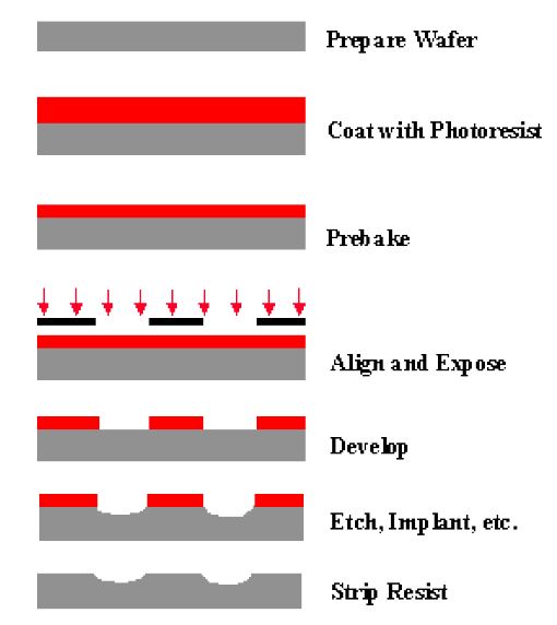
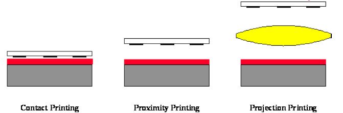 Figure: Lithographic printing in semiconductor manufacturing has evolved from contact printing (in the early 1960s) to projection printing (from the mid 1970s to today).
Contact and proximity lithography are the simplest methods of exposing a photoresist through a master pattern called a photomask (Figure above). Contact lithography offers high resolution (down to about the wavelength of the radiation), but practical problems such as mask damage and resulting low yield make this process unusable in most production environments. Proximity printing reduces mask damage by keeping the mask a set distance above the wafer (e.g., 20 μm). Unfortunately, the resolution limit is increased to greater than 2 to 4 μm, making proximity printing insufficient for today’s technology. By far the most common method of exposure is projection printing.
Projection lithography derives its name from the fact that an image of the mask is projected onto the wafer. Projection lithography became a viable alternative to contact/proximity printing in the mid 1970s when the advent of computer-aided lens design and improved optical materials allowed the production of lens elements of sufficient quality to meet the requirements of the semiconductor industry. In fact, these lenses have become so perfect that lens defects, called aberrations, play only a small role in determining the quality of the image. Such an optical system is said to be diffraction-limited, since it is diffraction effects and not lens aberrations which, for the most part, determine the shape of the image.
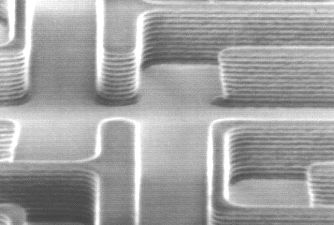
Another important aspect of photoresist exposure is the standing wave effect. Monochromatic light, when projected onto a wafer, strikes the photoresist surface over a range of angles, approximating plane waves. This light travels down through the photoresist and, if the substrate is reflective, is reflected back up through the resist. The incoming and reflected light interferes to form a standing wave pattern of high and low light intensity at different depths in the photoresist. This pattern is replicated in the photoresist, causing ridges in the sidewalls of the resist feature as seen in Figure 1-6. As pattern dimensions become smaller, these ridges can significantly affect the quality of the feature. The interference that causes standing waves also results in a phenomenon called swing curves, the sinusoidal variation in line width with changing resist thickness. These detrimental effects are best cured by coating the substrate with a thin absorbing layer called a bottom antireflective coating (BARC) that can reduce the reflectivity seen by the photoresist to less than 1 percent. The exposure parameters required in order to achieve accurate pattern transfer from the mask to the photosensitive layer depend primarily on the wavelength of the radiation source and the dose required achieving the desired properties change of the photoresist. Different photoresists exhibit different sensitivities to different wavelengths. The dose required per unit volume of photoresist for good pattern transfer is somewhat constant; however, the physics of the exposure process may affect the dose actually received. For example a highly reflective layer under the photoresist may result in the material experiencing a higher dose than if the underlying layer is absorptive, as the photoresist is exposed both by the incident radiation as well as the reflected radiation. The dose will also vary with resist thickness. There are also higher order effects, such as interference patterns in thick resist films on reflective substrates, which may affect the pattern transfer quality and sidewall properties.
Figure: Photoresist pattern on a silicon substrate showing prominent standing waves.
Original article by: Chris Mack
What equipment does Nanorian offers for this process?
Spin Coater by Laurell Corp.
Spin Coater by Laurell Corp.
Mask Aligner by Midas Corp.
Share
